Advanced Devices:LTCC Applied Devices
As of October 1, 2019, the LTCC Division was transferred to the joint venture company, LTCC Materials Co., Ltd.
Please visit the website here.
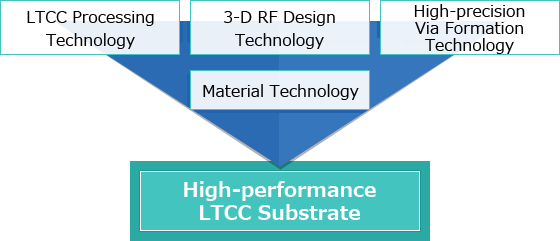
Developing new solutions harnessing LTCC and RF technology.
Yokowo's LTCC substrates and packages, sold the world over.
With the Low Temperature Co-fired Ceramics (LTCC) at the core, Yokowo offers LTCC substrates to enable high-density wiring, compatible with compact, low-back and RF devices.
LTCC: Ceramic Substrate
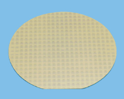
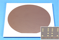 Wafer-level Chip Size Package Substrate (Self-developed material)
Substrates for use in the wafer level CSP sector increasingly require high-density, high-precision pattern formation and flatness. It is necessary to increase the size of substrates in the field of semiconductor testing equipment, while high heat release, high brightness and high durability are required in the field of LED packages. Yokowo harnesses cuttingedge LTCC processing technology and 3D RF design technology to offer its customers products that meet their needs with precision.
3-D RF Design
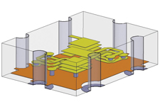 Using a circuit and electromagnetic field simulator, Ansoft Designer and HFSS, Yokowo provides circuit design and three-dimensional RF design for antennas, filters, RF module substrates and others.
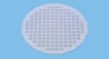
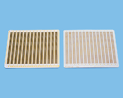
Interposer Substrate for Semiconductor Wafer Test
An LSI semiconductor wafer can have thousands of densely aligned bonding pads. LSI testing cannot be performed without a prober for physically expanding the narrow pitch pads of the semiconductor to connect them to the tester.
Based on its advanced LTCC processing technology, Yokowo has successfully developed an interposer substrate that plays a central role in the prober. Together with its vertical micro precision probe, Yokowo will respond to sophisticated demand from the semiconductor wafer sector.
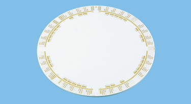
12 inch Interposer Substrate for Memory
(Internal Power Supply & Ground)
 Internal Wiring is Available
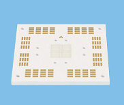 LTCC Interposer Substrate
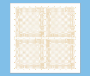 Enlarged DUT Pattern
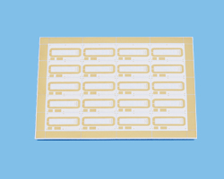
Interposer Substrate for Logic
(Multi Pin & Dut)
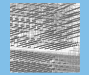 Radiograph of Stacked Via Holes(50 Layers, Via Dia. : 50µm)
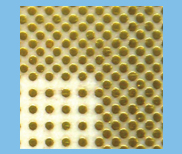 Fine Pitch Pad AreaMin. Pad Pitch : Around 120µm
LTCC Applied Devices
- LTCC Substrate for RF
- Dielectric Material for high frequency wave (εγ:50)
- Self-developed material: YDM-500 (US PAT No.7781359)
- Substrate for RF Module
- Dimensions of product: 3.3×5.1×0.5mm
- Printed Resistor: 1Ω~10MΩ
- LTCC Substrate Mounting High Frequency IC
- Mounting high frequency device
- LED LTCC Substrate
- High reflectance material
- High heat dissipation
- Excellent mountability due to its superior flatness
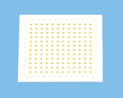
- LED Substrate for Vehicle
- Mounting high brightness LED
- LED Super-thin LTCC for CSP Substrate
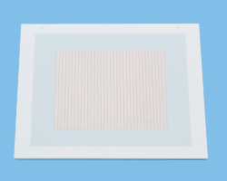
- Thickness : 0.075~0.150mm
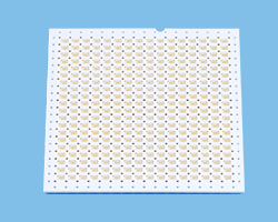
- Backlight LED Multiple LTCC Package
- LTCC Integral Structure
- The light that is more uniform than a package type
Other LTCC Product
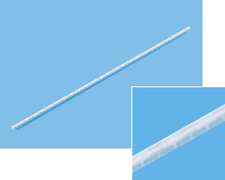
High Brightness/Ultraminiature LED RING LIGHT of LTCC
A compact size, high brightness, and extreme durability are requirements for the light sources of small CCD cameras. Yokowo has commercialized a High Brightness/Ultraminiature LED RING LIGHT of LTCC that fulfills these needs.
This product comes with multiple LED devices, is an ultraminiature size, and can be positioned directly under a small CCD camera without an optical fiber cable, and can secure a sufficient amount of light.
In addition, by adopting the heat resistant LTCC circuit board manufactured by Yokowo with its special silicon resin seal, this product has extreme durability.
Applications for use: dental instruments, industrial/medical endoscopes, microscopes, etc.
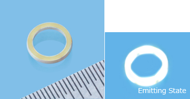
Scale=0.5mm